- Development and manufacturing of sensors for photon-counting computed tomography scanners
- Crystal growth on industrial scale
- Official opening ceremony with 300 guests
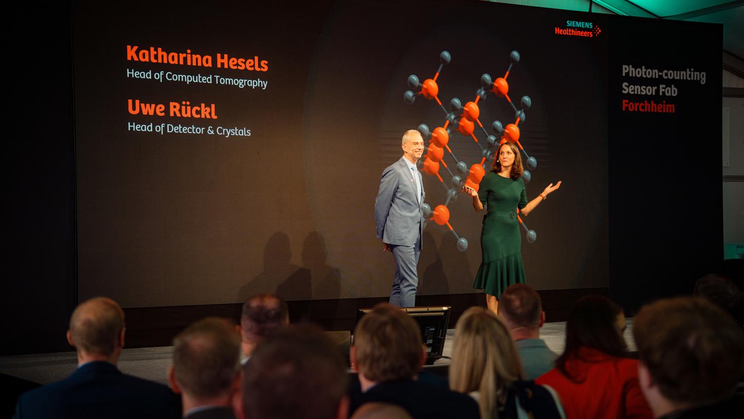
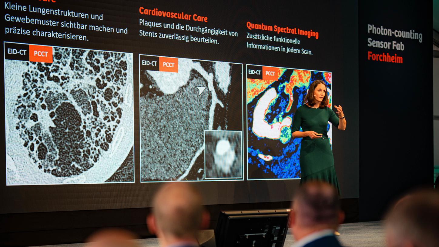
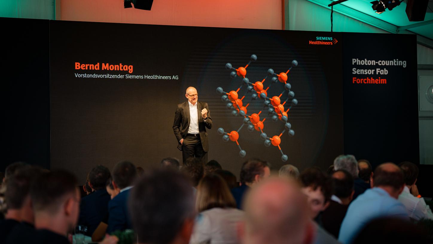
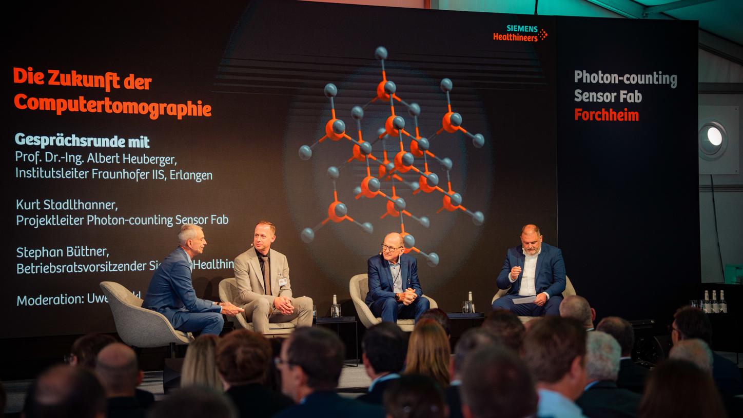
Siemens Healthineers today officially opened its semiconductor fabrication plant, the only facility of its kind in Europe, at its Forchheim site in Germany. The new Photon-counting Sensor Fab manufactures cadmium telluride (CdTe)-based semiconductor sensors for X-ray imaging. These sensors are used in photon-counting computed tomography (CT) scanners, enabling sharper images while potentially reducing radiation dose. At the opening ceremony, Bernd Montag, CEO of Siemens Healthineers, welcomed approximately 300 guests including representatives from politics and the healthcare sector, project partners, and employees. The facility, with approximately 9,500 square meters of usable floor space, will process cadmium and tellurium of the highest purity on an industrial scale. To ensure environmentally responsible handling of hazardous materials, Siemens Healthineers invested a single-digit million-euro amount in dedicated air emission and wastewater treatment systems. The company invested approximately €100 million in the construction and technical equipment of the facility and is creating more than 100 new jobs. Construction began in 2023 and has now been completed.
As demand for photon-counting CT scanners continues to grow, the existing Siemens Healthineers semiconductor sensor production facility in Japan is reaching its capacity limits. “We do not want to rely on a single-site strategy in Japan. We also want to be able to manufacture crystals on industrial scale here in Forchheim, at the center of CT development,” said Uwe Rückl, head of CT Detectors & Crystals at Siemens Healthineers. “Producing these sensors is complex and requires numerous individual process steps.” The Photon-counting Sensor Fab covers the entire manufacturing process, from graphite coating of quartz components and the formation of seed and polycrystals to controlled crystal growth. Cadmium and tellurium permanently bond only at temperatures of around 1,100 degrees Celsius. It takes approximately ten weeks for a cadmium-tellurium compound to develop into a single crystal. These crystals are then cut and polished with submillimeter precision before the pixel structure is applied lithographically in a cleanroom environment. The sensors are subsequently installed in photon-counting CT scanners at the company’s CT manufacturing facility.
The new building in Forchheim has achieved LEED Platinum certification and is operated in a sustainable, carbon-neutral manner. For example, heat generated during production is used to heat the building, while a rooftop photovoltaic system with a capacity of 170 kWp generates renewable electricity on site. Environmentally conscious landscaping, light-colored sealed surfaces, and shade-providing vegetation help prevent the heat island effect and the building from overheating. Siemens Healthineers selected native plant species suited to the location to promote local biodiversity. This is complemented by an innovative LED lighting concept, while reduced lighting in the outdoor areas minimizes light pollution and helps protect nocturnal wildlife.
Further information on photon-counting CT can be found here: https://www.siemens-healthineers.com/en-us/computed-tomography/ct-technologies-and-innovations/photon-counting-ct.